|
|
|
|
|
|
Product Details:
Payment & Shipping Terms:
|
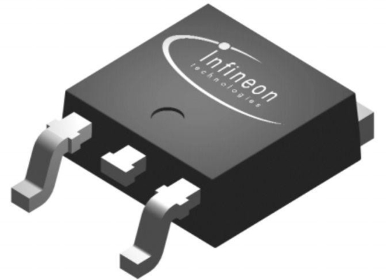
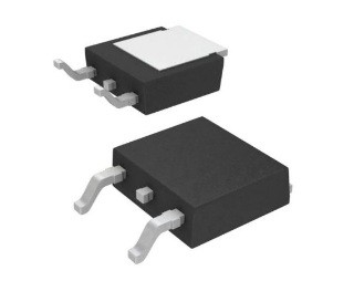
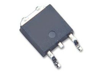
| MPN: | IPD90R1K2C3 | MFR: | Infineon |
|---|---|---|---|
| Category: | Mosfet | Size: | 2.41*6.73*6.22mm |
| Highlight: | IPD90R1K2C3 High Power MOSFET,High Power MOSFET 3 Pin,AMPAK Wifi Module N-CH |
||
| EU RoHS | Compliant with Exemption |
| ECCN (US) | EAR99 |
| Part Status | Active |
| SVHC | Yes |
| SVHC Exceeds Threshold | Yes |
| Automotive | No |
| PPAP | No |
| Product Category | Power MOSFET |
| Configuration | Single |
| Process Technology | CoolMOS |
| Channel Mode | Enhancement |
| Channel Type | N |
| Number of Elements per Chip | 1 |
| Maximum Drain Source Voltage (V) | 900 |
| Maximum Gate Source Voltage (V) | ±20 |
| Maximum Gate Threshold Voltage (V) | 3.5 |
| Operating Junction Temperature (°C) | -55 to 150 |
| Maximum Continuous Drain Current (A) | 5.1 |
| Maximum Gate Source Leakage Current (nA) | 100 |
| Maximum IDSS (uA) | 1 |
| Maximum Drain Source Resistance (MOhm) | 1200@10V |
| Typical Gate Charge @ Vgs (nC) | 28@10V |
| Typical Gate Charge @ 10V (nC) | 28 |
| Typical Input Capacitance @ Vds (pF) | 710@100V |
| Maximum Power Dissipation (mW) | 83000 |
| Typical Fall Time (ns) | 40 |
| Typical Rise Time (ns) | 20 |
| Typical Turn-Off Delay Time (ns) | 400 |
| Typical Turn-On Delay Time (ns) | 70 |
| Minimum Operating Temperature (°C) | -55 |
| Maximum Operating Temperature (°C) | 150 |
| Packaging | Tape and Reel |
| Maximum Positive Gate Source Voltage (V) | 20 |
| Maximum Diode Forward Voltage (V) | 1.2 |
| Pin Count | 3 |
| Standard Package Name | TO-252 |
| Supplier Package | DPAK |
| Mounting | Surface Mount |
| Package Height | 2.41(Max) |
| Package Length | 6.73(Max) |
| Package Width | 6.22(Max) |
| PCB changed | 2 |
| Tab | Tab |
| Lead Shape | Gull-wing |
Contact Person: peter
Tel: +8613211027073